Scanning electron microscope
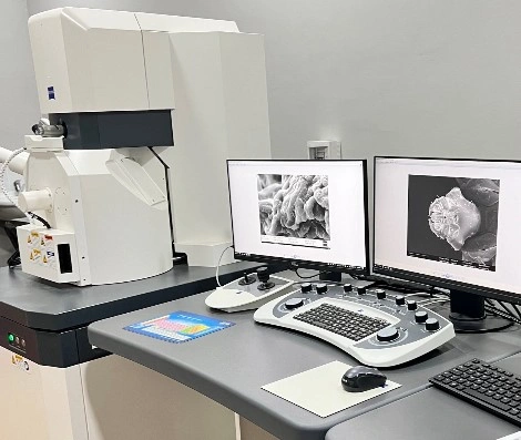
The Institute is equipped with a modern scanning electron microscope (SEM) - the Zeiss EVO 15 - featuring SE, BSE, and EDX detectors and a tungsten filament. This instrument is designed for high-precision imaging of the structure of both organic and inorganic materials. With its extensive imaging mode capabilities, the microscope is actively used in both scientific research and applied projects.
Scanning Electron Microscopy is a high-resolution method for imaging object surfaces using an electron beam. Unlike optical microscopes, SEM allows for the visualization of micro- and nanostructures with exceptional detail. Images are formed through the interaction of electrons with the sample surface, providing outstanding clarity and depth of field.
This method allows for:
- Studying surface morphology and topography
- Analyzing the microstructure of tissues, materials, and coatings
- Performing elemental analysis
- Detecting defects, microcracks, and contaminants
We offer scanning electron microscopy services for scientific, medical, industrial, and educational institutions. At our Institute, we follow modern protocols for preparing organic samples, including:
- Biological tissues (e.g., organ fragments, cells, extracellular matrices)
Our services include:
- Sample preparation (fixation, dehydration, metal coating)
- Imaging in SE or BSE mode (secondary and backscattered electrons)
- Quantitative and qualitative elemental analysis (EDX)
- Reporting and consulting on image interpretation